You can search for courses, events, people, and anything else.
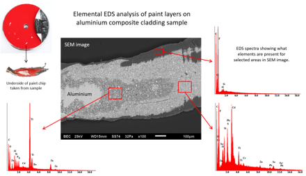
All AMCF Scanning Electron Microscopes are equipped with Energy Dispersive Spectroscopy (EDS) detectors for elemental microanalysis and X-ray mapping (XRM). These detectors allow us to generate an EDS spectrum, which is a spectrum of the x-ray energies emitted from a spot or an area of a sample. As every element has specific characteristic X-ray energies, we are able to determine a sample’s elemental composition. If the sample is prepared properly, results can be both qualitative and quantitative.
X-ray Mapping (XRM) is the collection of characteristic X-rays as a function of the position of the scanning electron beam on the sample. In other words, we are collecting an EDS spectrum for each pixel in an SEM image. Using an XRM software package, we are then able to extract data from all of the spectra collected, and colour code each pixel in an image to show what elements are present.
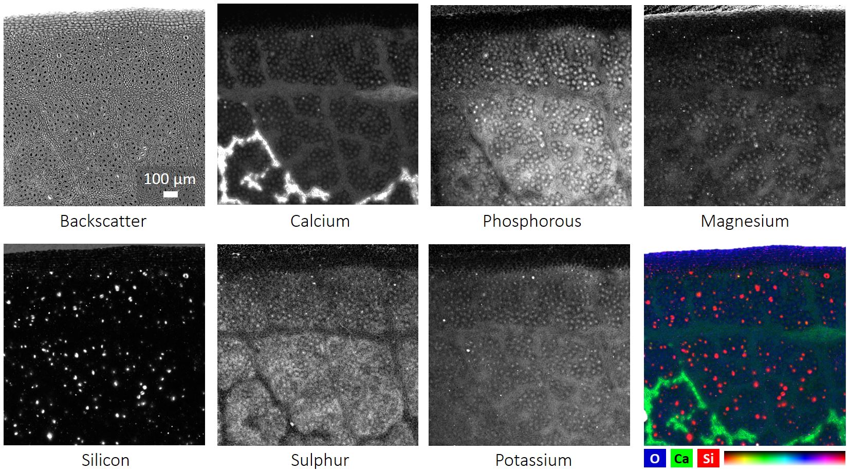
A backscatter SEM image of a Eucalyptus leaf (top left), and some of the corresponding elemental XRM maps collected. Bottom left shows a false coloured image, where elements have been assigned a colour. This allows us to now spatially locate where elements are in a sample.
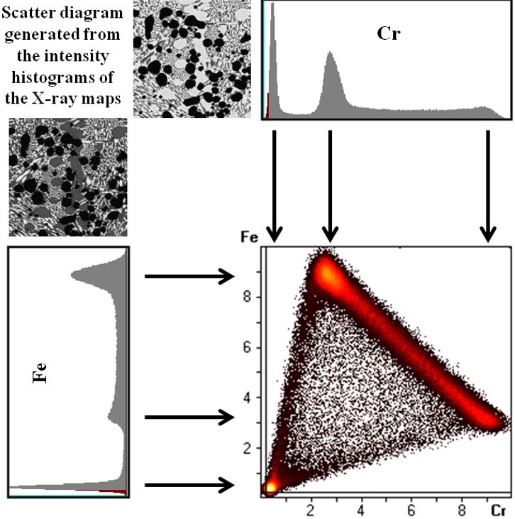
The X-ray intensity distributions of the elements from an X-ray map allow us to generate two dimensional and ternary scatter diagrams, converting spatial information into concentration dimensions. This is an important tool for displaying the spatial relationships of elements or correlated elements (phases) in materials. The method to accomplish this is through the use of two and three-dimensional (2D and 3D) scatter (or correlation) diagrams, which are generated from the X-ray maps.
From these scatter diagrams we observe clusters, also referred to as nodes, which correspond to different chemical phases. We can also observe linking (connection) between clusters indicating the boundaries between phases within a material as well as branching from clusters (some links may contain branches).
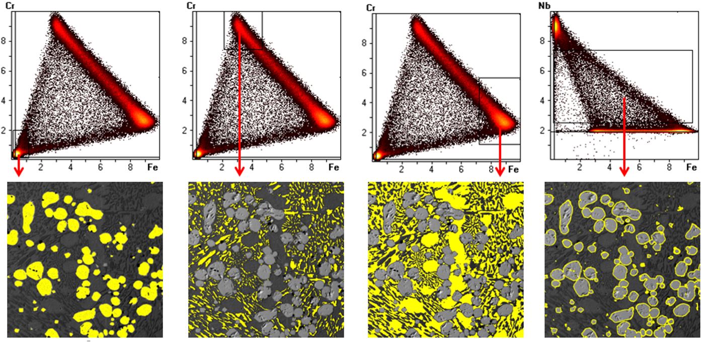
Generation of scatter diagrams for a white cast iron hard-facing material with NbC particles. A set of scatter diagrams for iron versus chromium (a-c) and niobium versus iron (d) showing different cluster selections and the corresponding points then displayed and redrawn on the SEM image.
From the clusters observed in the scatter diagram, it is possible to map the phases. This is often referred to as phase mapping, but really it should be called chemical phase mapping (CPM), as phase mapping assumes knowledge of crystal structure and requires diffraction analysis.
Chemical phase mapping (CPM) involves selecting areas on the scatter diagrams and observing where the points or clusters relate on the BSE image and is an important part of the phase identification process. These selected analysis points may then be summed for a more accurate analysis in total or by selecting strategic areas on the image.
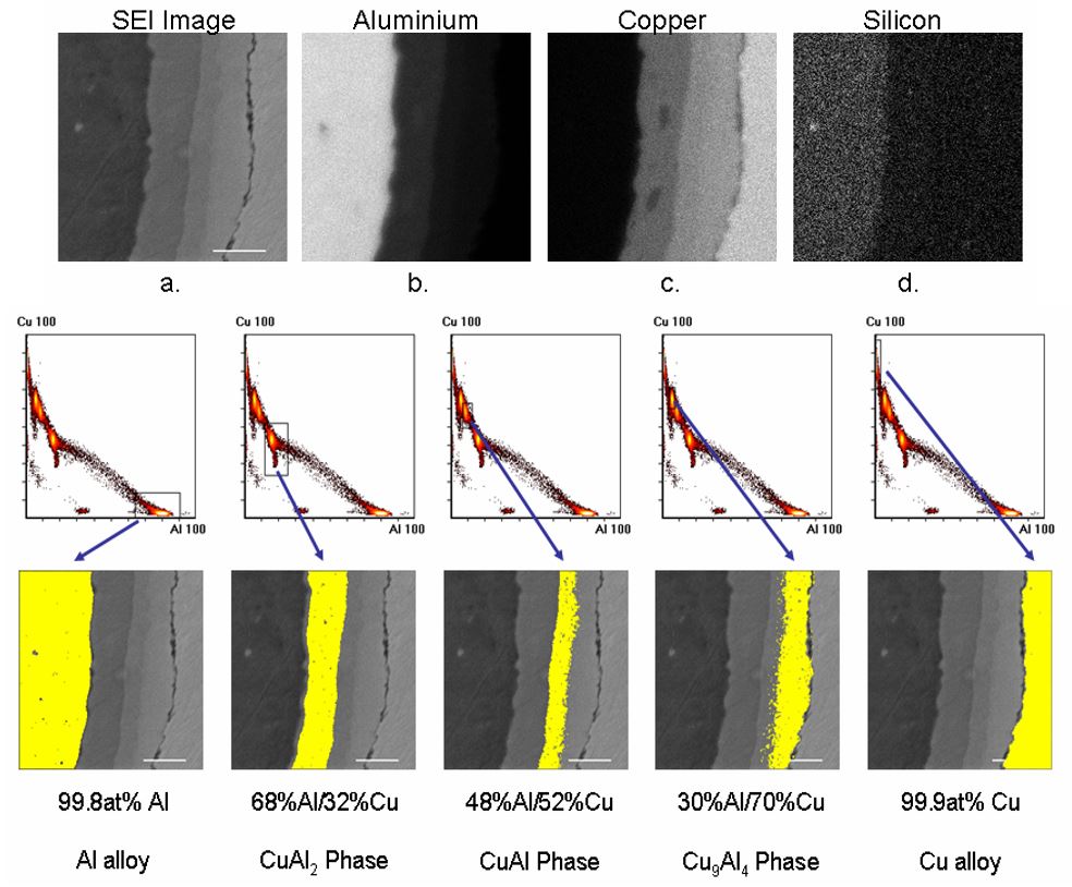
BSE, XRM and scatter diagrams for copper-aluminium laminate. The images at the bottom are secondary electron images with information from the different clusters of the scatter diagram superimposed over the image
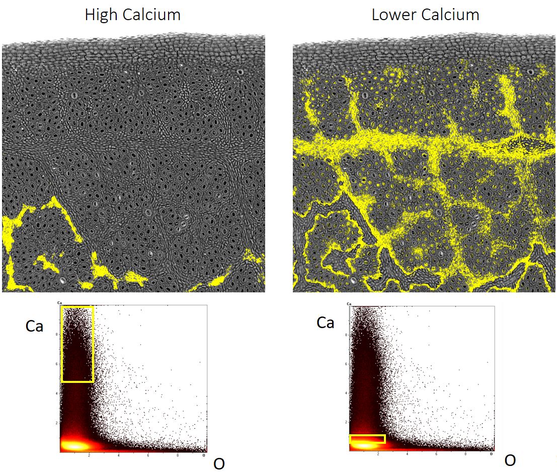
Superimposed BSE images of a Eucalyptus leaf, showing the presence of high and low amounts of calcium in the leaf. This has been done using the information taken from teh scatter diagrams below. The high amounts show where calcium oxalate crystals have formed just below the leaf’s surface.