You can search for courses, events, people, and anything else.
The AMCF has a number of Scanning Electron Microscopes (SEM) available for use, all of which are equipped with Secondary Electron (SE) and Backscatter Electron (BSE) detectors for imaging, and Energy Dispersive Spectroscopy (EDS) detectors for elemental microanalysis (see section on Microanalysis & Mapping). Two of our instruments also have Scanning Transmission Electron Microscopy (S-TEM) capabilities. Depending on your imaging and analysis needs, we also have a number of specialist holders, detectors and techniques which can be used, and a full range of sample preparation equipment, including coaters, resin mounting, grinding and polishing, critical point drying, microtomes and more (see Supporting Equipment).
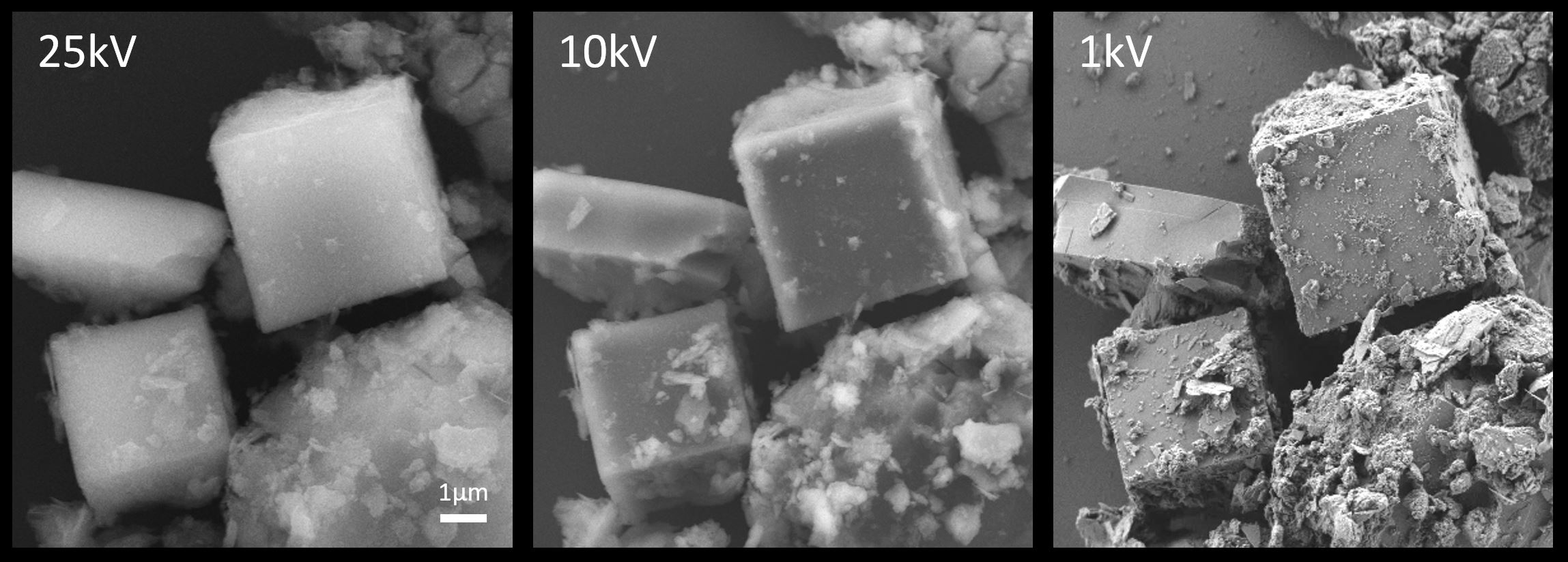
A sample imaged with a secondary electron detector at different accelerating voltages (kV). Higher accelerating voltages are usually needed for elemental microanalysis, but lower kV’s can give more detail of sample surfaces.
Available detectors
Secondary Electron (SE) detector
All SEMs
General imaging under high vacuum.
Backscatter Electron (BSE) detector
All SEMs
Low vacuum imaging of fresh or uncoated samples. Shades of grey also give information on where high and low atomic mass elements or phases are located.
Energy Dispersive Spectroscopy (EDS) detector
All SEMs
Elemental microanalysis of samples for identification, and X-ray mapping (XRM) for spatially locating elements and phases.
InLens detector
Zeiss Merlin, Jeol 7001 SEMs
Great for imaging at low accelerating voltages, where small surface features are of interest.
Scanning Transmission Electron Microscopy (S-TEM) detector
Zeiss Merlin, Jeol 7001 SEMs
Transmission imaging of sample sections on grids.
Ultra Variable pressure Detector (UVD)
Hitachi FlexSEM
A secondary detector which can be used under low vacuum with fresh or uncoated samples.
Cathode Luminescence (CL) imaging detector
Zeiss Merlin, Hitachi FlexSEM
Imaging of sample areas which emit light.
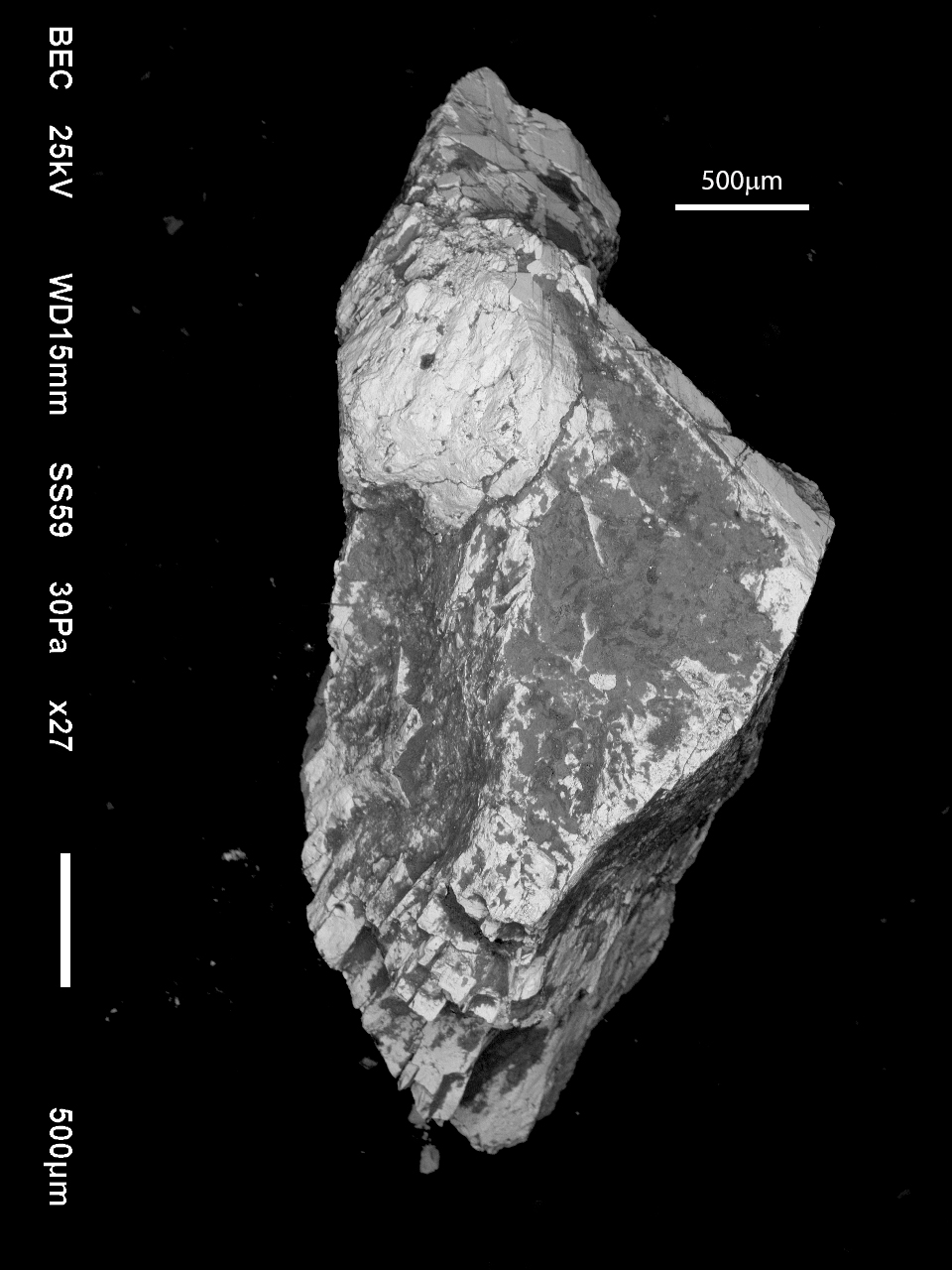
Backscatter image of a mineral. The bright patches show that there is a heavier element present in these areas, while the darkers areas show the presence of lighter elements.
Jeol JSM 6510LV SEM
Source: Tungsten (W) electron filament.
Vacuum: High and variable low vacuum modes.
Stage Control: Manual 5-axes stage (X, Y, Z, Tilt and Rotate).
Accelerating Voltages: 1 - 30kV
Imaging Detectors: Secondary and Backscatter.
Microanalysis Detector: Amptek SSD C1 EDS detector, supported by Moran Scientific software package for X-ray analysis of elements present (EDS).
Advantages: A great workhorse, good for initial sample examination. This SEM is useful for natural state analysis in low vacuum, requiring minimal or no sample preparation. Its large chamber is great for analysis of bigger samples.
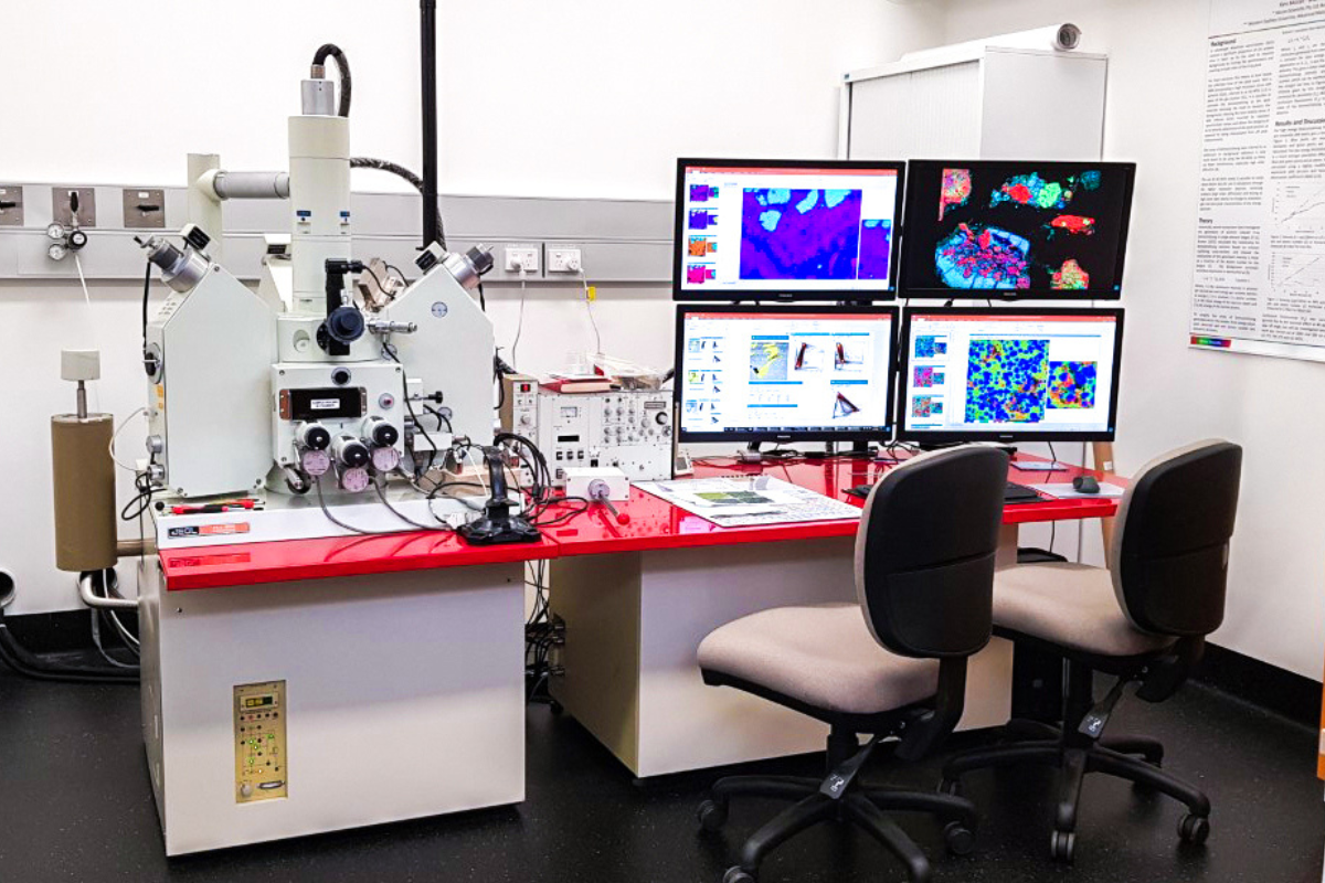
Zeiss Merlin Compact VP SEM
Source: Schottky Field Emission Gun (FEG).
Vacuum: High and variable low vacuum modes.
Stage Control: Motorized 5-axes stage (X, Y, Z, Tilt, Rotate).
Accelerating Voltages: 0.1 - 30kV.
Imaging Detectors: Secondary, Backscatter, InLens, S-TEM (transmission imaging) and CL detectors.
Microanalysis Detector: Bruker Quantax EDS detector, supported by Bruker Espirit software package
Advantages: With its large range of electron energies and specialty detectors, anything from detailed surface analysis to scanning transmission imaging is possible. Surrounded by a magnetic field compensation system allowing greater field stability, the Zeiss is capable of high resolution and high magnification imaging (up to 2 million times possible), great for work on nano-materials.
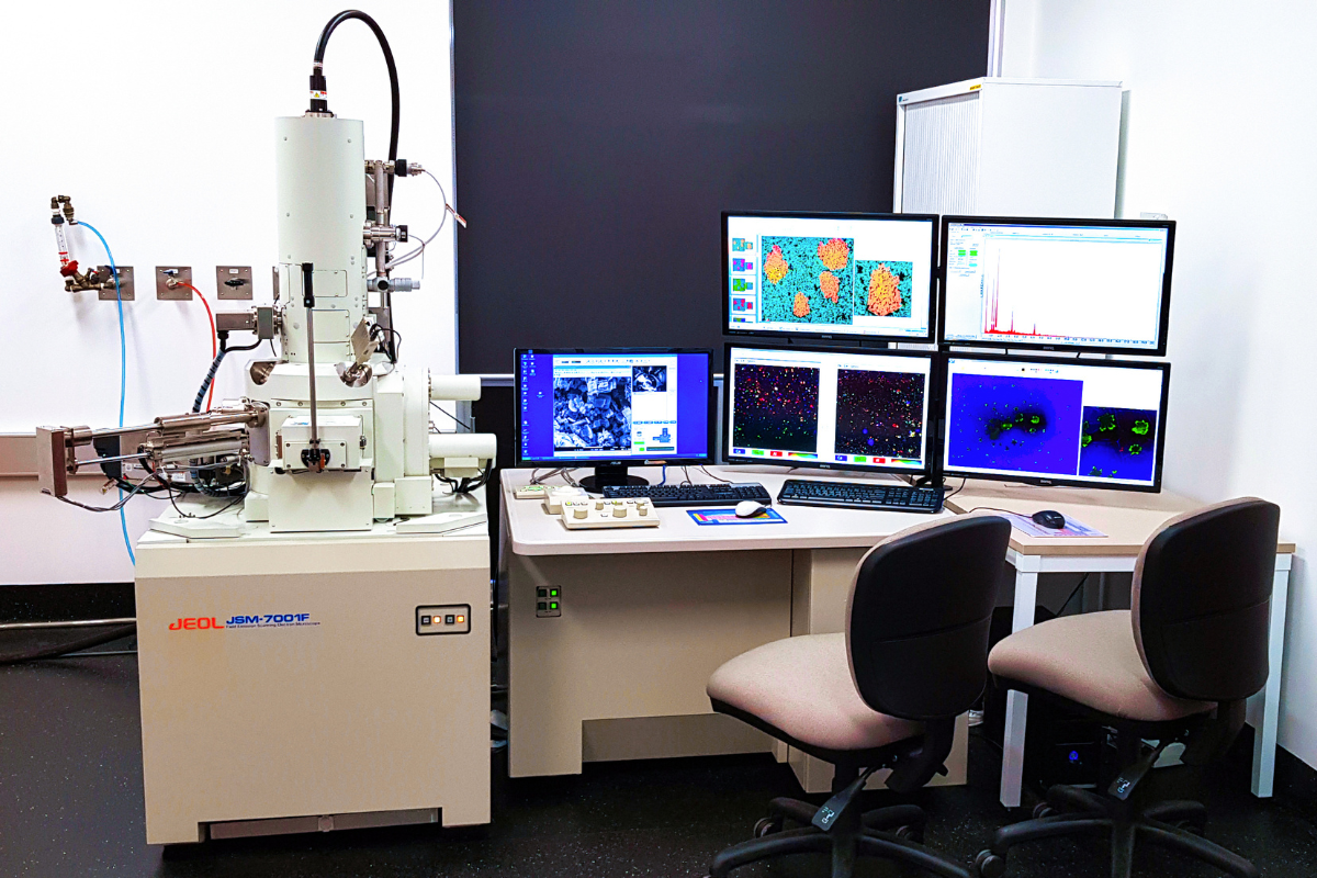
Jeol JSM 7001FEG SEM
Source: Schottky Field Emission Gun (FEG)
Vacuum: High vacuum.
Stage Control: Motorized 5-axes stage (X, Y, Z, Tilt, Rotate)
Accelerating Voltages: 1 - 30kV
Imaging Detectors: Secondary, Backscatter, InLens and S-TEM (transmission imaging) detectors.
Microanalysis Detector: Multiple Amptek SSD EDS detectors, supported by Moran Scientific software package for X-ray analysis of elements present (EDS) and X-ray Mapping (XRM)
Advantages: With a FEG electron source, multiple EDS detectors and the latest Moran Scientific software, this instrument specialises in producing high quality X-ray Mapping images of prepared samples.
Jeol JXM 8600 Probe
Source: Tungsten electron filament.
Vacuum: High vacuum.
Stage Control: Motorized 5-axes stage (X, Y, Z, Tilt, Rotate)
Accelerating Voltages: 1 - 49kV
Imaging Detectors: Secondary and Backscatter.
Microanalysis Detectors: Amptek SSD C2 EDS detector and Wavelength Dispersive Spectroscopy (WDS) detector. Both are supported by Moran Scientific software package for X-ray analysis of elements present (EDS/WDS) and X-ray Mapping (XRM)
Advantages: Designed for non-destructive X-ray microanalysis and imaging of solid materials. Capable of high spatial resolution and relatively high analytical sensitivity. Has WDS capability for trace elemental analysis.
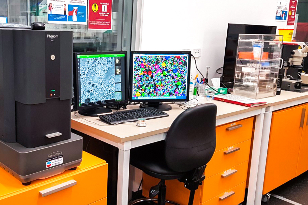
Phenom XL Desktop SEM
Source: Cerium Hexaboride (CeB6) electron filament.
Vacuum: High and set low (10 and 60Pa) vacuum.
Stage Control: 3-axes stage (motorised X-Y, and manual Z). Does have scan rotation in software.
Accelerating Voltages: 5 - 15kV
Imaging Detectors: Secondary and Backscatter.
Microanalysis Detectors: EDS detector supported by both the Phenom Pro-suite and the Moran Scientific microanalysis and X-ray mapping software packages.
Advantages: Small, portable and highly capable. The Phenom SEM includes optical microscope imaging for stage navigation. The Phenom Pro-Suite package includes software for elemental analysis, particle/pore sizing, image stitching and surface roughness analysis. Its large stage which can hold over 20 samples is an added bonus.
Hitachi FlexSEM
Source: Tungsten electron filament.
Vacuum: High and variable low vacuum modes.
Stage Control: 5-axes stage (motorised X-Y, and manual Z, tilt and rotation).
Accelerating Voltages: 5 - 20kV
Imaging Detectors: Secondary, UVD and Backscatter.
Microanalysis Detectors: Bruker Quantax EDS detector, supported by Bruker Espirit software package.
Advantages: The Ultra Variable-pressure Detector (UVD) allows for high resolution SE imaging of uncoated samples in their natural state in low vacuum mode. With optical microscope imaging for stage navigation this SEM is easy to use.